For a sensor, the amount of harmful exposure it receives from the environment and harmful constituents in the measuring process depends on what is being sensed and the environment itself. Different packaging is required to cope with and survive the specific situation. Two major considerations for protection are at the sensing element/transducer level or at the sensing module level.
Today, microelectromechanical systems (MEMS) technology provides many different types of sensing/transducer elements. MEMS sensors are based on integrated circuit/semiconductor processing. The differences in MEMS sensor packaging depends on sensors that are isolated from the environment and those that must specifically interact and come in contact with the measurand.
At the silicon level for MEMS devices, packaging approaches/technologies included over molded, exposed die surface and cavity designs. Packaging materials are commonly plastic for high-volume applications and for more demanding applications, metal can and ceramic materials are used.
In a factory environment, a sealed sensor package with minimum exposure to harsh chemicals, such as a sensor mounted on a printed circuit board inside a module designed for the environment, may strictly rely on a high-volume plastic package.
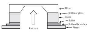
In contrast, a sensor that must contact a media such as water has different design considerations. For example, when a pressure sensors must interface to substances beyond dry air, one common recommendation is measuring the pressure from the back side. The top side of the pressure sensor die has the sensing elements and potentially other circuitry that cannot survive exposure to water. As shown in the figure, the sensor can survive in the application as long as the media providing the backside pressure does not have a detrimental impact to the silicon, plastic and other materials in the sensing element stack.
Materials impacted by applying back-side pressure. Source: Understanding Smart Sensors, 3rd Edition.
One of the common solutions for isolating the top surface of a pressure sensor is a protective coating such as parylene that is applied by a vapor deposition polymerization process. The parylene allows pressure to be transmitted to the top side of pressure sensor.
At the module or end-packaging level, epoxy encapsulation and O-rings for sealing are among the packaging techniques used to provide increased protection to a sensor.
To address the harshest applications where an IP69K rating is required, the materials get rather specific. The packaging housing is frequently a hermetically-sealed stainless steel such as 316, or an FDA-grade with a molded connector to attach to an external cordset/cable.
Polybutylene terephthalate (PBT) thermoplastic housing or cast aluminum housing can also be found as packaging materials for IP69K rated sensors.
These are just a few of the examples of matching the sensor’s packaging capabilities to its application requirements. In many cases, a sensor supplier may have extensive knowledge of its sensors’ capabilities to survive specific applications.

