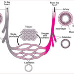
The previous part of this article looked at the challenges of nanoflow sensors, especially with respect to blood flow. This part looks at graphene, which is the basis for the new sensor.
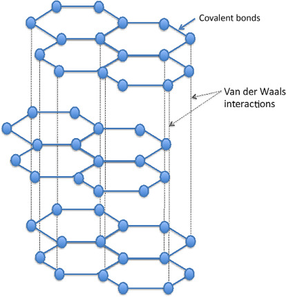
Graphene is a material structure which did not exist until relatively recently. However, its constituent element of graphite – the crystalline form of the element carbon with its atoms arranged in a hexagonal structure (Figure 1) – has been known and used for centuries and has countless uses in consumer products, industrial production, and yes, even pencil “lead.” Other allotropes of carbon are diamonds, of course, as well as carbon nanotubes and fullerenes, all fascinating structures. (An allotrope represents the different physical forms in which an element can exist; graphite, charcoal, and diamond are all allotropes of carbon.)
While graphene is composed of graphite, it’s a very special form of that element. Graphene is a monolayer form of graphite, as a one-atom-thick (or “thin”) layer of carbon atoms bonded to each other and arranged in a hexagonal or honeycomb lattice (Figure 2).
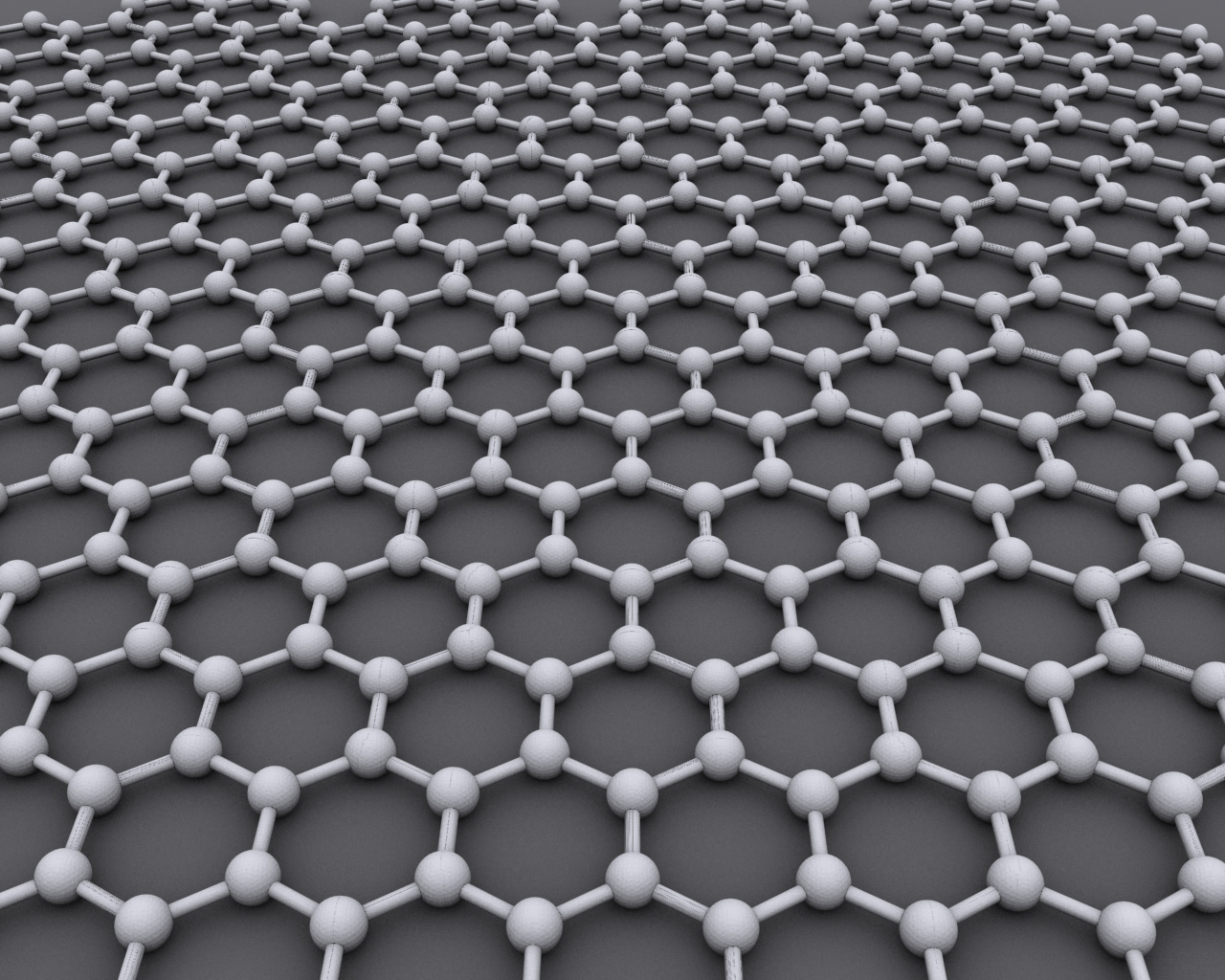
That sounds like “no big deal” or “no important difference,” but that is not the case at all. Graphene is the thinnest material known to man at one atom thick and also incredibly strong – about 200 times stronger than steel. On top of that, graphene is an excellent conductor of heat and has interesting light absorption abilities. As a conductor of electricity, it performs better than copper. It is almost completely transparent yet so dense that not even helium, the smallest gas atom, can pass through it. Graphene is a mere one atom thick– perhaps the thinnest material in the universe–and forms a high-quality crystal lattice with no vacancies or dislocations in the structure. This structure gives it intriguing properties and yielded surprising new physics.
There’s some irony associated with graphene. While carbon has been known and used “forever” (so to speak), graphene itself is relatively new. Although scientists knew that one-atom-thick, two-dimensional crystal graphene could exist in theory, no one had worked out how to extract or create it from graphite.
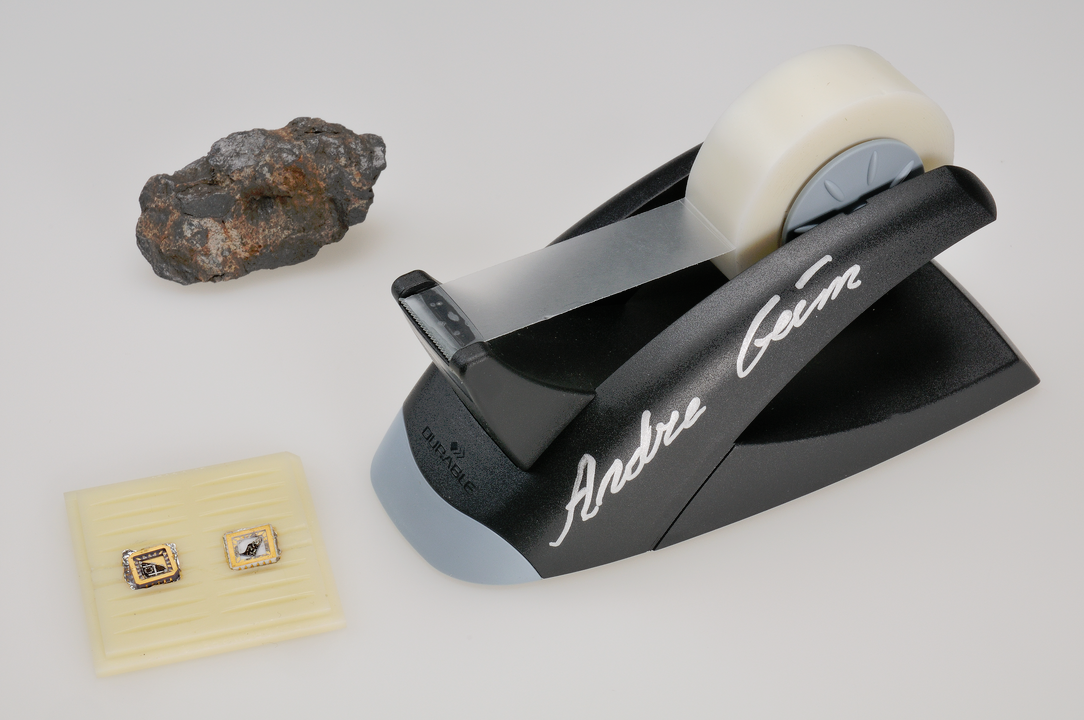
However, in 2004, researchers Professor Andre Geim and Professor Kostya Novoselov (both Russian-born but working as researchers at The University of Manchester, UK), first isolated graphene by peeling graphite into thinner and thinner layers by repeatedly using “Scotch” adhesive tape, then dissolving the tape itself, Figure 3 (there’s obviously much more to this story). The pair received the Nobel Prize in Physics for 2010 for their theoretical and applied work, which was presented in their paper “Electric Field Effect in Atomically Thin Carbon Films” published in Science.
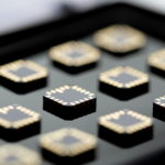
It would be easy to say, “graphene sounds nice and even somewhat interesting, but so what?” but there is much more to it. In many ways, it is like silicon in that it has many “undiscovered” uses and is almost a wonder substance, solving potential problems on its own or in combination with other materials. Figuring out how to make it as a standard, almost mass-produced product was another challenge, but you can now buy it as fibers and in sheets from specialty supply houses.
In some ways, application ideas for graphene are analogous to the laser. When Theodore H. Maiman first demonstrated the laser to the press and public in 1960, the “quip” among journalists was that the laser was “a solution looking for problems to solve.” We certainly know how that mystery story has turned out, and graphene, too, has found its way into many applications.
One application uses graphene to replace silicon-based transistors since that technology is fast reaching its fundamental limits (below 10 nanometers). It is also possible to make graphene using epitaxial growth techniques – growing a single layer on top of crystals with a matching substrate – to create graphene wafers for electronics applications such as high-frequency transistors operating in the terahertz region or to build miniature printed circuit boards at the nanoscale.
Graphene is being used as a filler in plastic to make composite materials, in reinforced tennis and other racquets, for example. Graphene suspensions can also be used to make optically transparent and conductive films suitable for LCD screens. Finally, it can also be the basis for unique sensors such as the nanoflow project discussed in Part 3. As an added benefit, elemental graphite, graphene, and other carbon-based structures are not considered health hazards in general or to the body in particular. (Do not confuse “carbon” with “carbon dioxide”, often cited in relation to climate change – that sloppy terminology has most people using the single word “carbon” when what they really mean is the carbon dioxide CO2 molecule, which is a completely different substance.)
EE World Related Content
- Graphene solid state devices – What does the future hold?
- AstroSlide 5G phone: Electronics and graphene will make it run
- Coriolis flowmeters: A subtle global effect with local applications, Part 1: The challenge
- Coriolis flowmeters, Part 2: The principle
- Coriolis flowmeters, Part 3: Flowmeter design
- Coriolis flowmeter, Part 4: The future
- Magnetic resonance imaging (MRI), Part 1: How it works
- MRI, Part 2: Historical development (and lawsuits)
- TT Electronics’ Self-Calibrating Fluid Sensors Enable Engineers to Easily Correct for System Variations
- Wafer-based Tunneling Magnetoresistive analog sensor targets fluid measurement apps
- The working principle, applications and limitations of ultrasonic sensors
External References
Graphene related
- Encyclopædia Britannica, Inc., “Graphite”
- Graphene Info, “What is Graphene?”
- Manchester University, National Graphene Institute (NGI)
- Scientific American, “Carbon Wonderland” (2008)
- APS News, “Discovery of Graphene” (2004)
- Science, “Electric Field Effect in Atomically Thin Carbon Films” (2004) (behind a paywall)
- ResearchGate, “Electric Field Effect in Atomically Thin Carbon Films” (no paywall)
- YouTube, “Electric Field Effect in Atomically Thin Carbon Films” (20-minute video)
Flow Sensor related
- Nature Communications, “Flow-sensory contact electrification of graphene” (pdf)
- Nature Communications, “Flow-sensory contact electrification of graphene” (non-pdf web version)
- Nature Communications, “Supplementary Information”
- Untitled 30-second video plus caption of the video
- University of Massachusetts, “UMass Amherst Researchers Develop Ultra-Sensitive Flow Microsensors”