• Skip to primary navigation
  • Skip to main content
  • Skip to primary sidebar
  • Skip to footer
  • Subscribe
  • Advertise

Sensor Tips

Sensor Product News, Tips, and learning resources for the Design Engineering Professional.

  • Motion Sensing
  • Vision systems
    • Smart cameras
    • Vision software
    • Lighting
    • Optics
  • Pressure
  • Speed
  • Temperature
  • Suppliers
  • Video
    • EE Videos
    • Teardown Videos
  • EE Learning Center
    • Design Guides
    • Tech Toolboxes

How do you get your sensing idea into production?

June 25, 2019 By Randy Frank

If the idea is already in the design phase, you may just be looking for a company that will manufacturer (fabricate or fab) your device. The choice of a fab involves different criteria including, of course, cost.  In addition to the wafer fabrication packaging is also a major consideration.

A fab process that allows wafer level processing of both the microelectromechanical systems (MEMS) sensor and the associated circuitry would be highly advantageous.

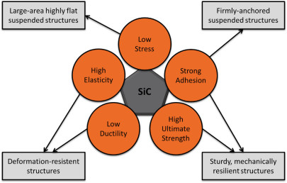
Unlike processes that build MEMS devices before or beside the electronics on the same die, a process that grows MEMS devices above the IC without any having side effects on the electronics underneath has advantages.  This results in smaller die sizes, higher performance for many applications, as well as higher levels of integration. One company that achieves MEMS devices above the IC is MEMS VISION. Through the company’s MoSiC™ process that uses silicon carbide instead of silicon, they can deliver higher elastic modulus, higher acoustic velocity, higher temperature resistance, higher ultimate strength, inert surfaces and higher resistance to wear.

With the close integration of MEMS and the IC, they can produce sensors with very high sensitivity, very high speed and minimum power consumption. For those applications that are less demanding, the MEMS devices can be fabricated separately and then coupled with the electronic die in a system-in-package (SiP) solution with multiple dies or even as two distinct chips. The fabrication of the MEMS devices can be done at the company’s fab partner or the process can be performed at a fab that the user chooses. Not all customers will meet the company’s criteria to take advantage of their approach but with all of the potential advantages, it certainly is worth exploring.

Filed Under: Featured, Frequently Asked Question (FAQ) Tagged With: MEMS VISION

Primary Sidebar

Featured Contributions

A2L refrigerants drive thermal drift concerns in HVAC systems

Integrating MEMS technology into next-gen vehicle safety features

Fire prevention through the Internet

Beyond the drivetrain: sensor innovation in automotive

Sensors in American football can help the game

More Featured Contributions

EE TECH TOOLBOX

“ee
Tech Toolbox: 5G Technology
This Tech Toolbox covers the basics of 5G technology plus a story about how engineers designed and built a prototype DSL router mostly from old cellphone parts. Download this first 5G/wired/wireless communications Tech Toolbox to learn more!

EE LEARNING CENTER

EE Learning Center
“sensor
EXPAND YOUR KNOWLEDGE AND STAY CONNECTED
Get the latest info on technologies, tools and strategies for EE professionals.

RSS Current EDABoard.com discussions

  • Snooping Around is All
  • mosfet driver problem in regeneration mode
  • Industrial Relay Board Design for Motorcycle Use
  • connector model question
  • ADEM III ECM — No CAN Signal & Power Supply Issue

RSS Current Electro-Tech-Online.com Discussions

  • Sump pit water alarm - Kicad 9
  • Pic18f25q10 osccon1 settings swordfish basic
  • Anyone jumped from Easyeda std to Easyeda pro?
  • turbo jet fan - feedback appreciated.
  • More fun with ws2812 this time XC8 and CLC

EE ENGINEERING TRAINING DAYS

engineering
“bills

RSS Featured White Papers

  • 4D Imaging Radar: Sensor Supremacy For Sustained L2+ Vehicle Enablement
  • Amphenol RF solutions enable the RF & video signal chains in industrial robots
  • Implementing Position Sensors for Hazardous Areas & Safety

DesignFast

Component Selection Made Simple.

Try it Today
design fast globle

Footer

EE WORLD ONLINE NETWORK

  • 5G Technology World
  • EE World Online
  • Engineers Garage
  • Analog IC Tips
  • Battery Power Tips
  • Connector Tips
  • DesignFast
  • EDA Board Forums
  • Electro Tech Online Forums
  • EV Engineering
  • Microcontroller Tips
  • Power Electronic Tips
  • Test and Measurement Tips

SENSOR TIPS

  • Subscribe to our newsletter
  • Advertise with us
  • Contact us
  • About us

Copyright © 2025 · WTWH Media LLC and its licensors. All rights reserved.
The material on this site may not be reproduced, distributed, transmitted, cached or otherwise used, except with the prior written permission of WTWH Media.

Privacy Policy