A transition edge sensor (TES) is a microcalorimeter based on superconductivity. Compared with alternative technologies like energy dispersive X-ray spectroscopy (EDS), a TES can provide higher resolution measurements and resolve emission lines at closely adjacent energies. In astrophysics, TES is used to measure the relative abundance of elements like boron, carbon, and oxygen versus silicon to develop information about the solar wind effect and for studies related to the origin of water on Earth.
A TES converts individual photons into heat pulses and measures their energy. They use the narrow superconducting-to-normal state transition region of a thin metal film. The transition region is typically about a milliKelvin (mK). A TES can measure temperature changes under 1 microKelvin (μK).
A superconductor’s resistance drops quickly to zero at its critical temperature (Tc). A bias current in the thin-film superconductor keeps it in the transition region between its normal and superconducting states (blue dot in Figure 1). When a photon is absorbed, the superconductor is heated by an amount ∆T proportional to the energy in the photon, indicated by the blue arrow. The change in current is measured, and the temperature change can be calculated.
By optimizing the materials, temperature, and size of the TES, it can be designed to measure the energy of single photons from optical to gamma-ray wavelengths. There’s a variety of superconducting metal films available for TES. In the TES described in Figure 1, molybdenum/gold (Mo/Au) bilayers were used. The thin films use the proximity effect, where the two metals operate as if they are a single film. By controlling the bilayer structure, the Tc can be controlled between 800 mK (the Tc of Mo) and 0 K (the Tc of Au).
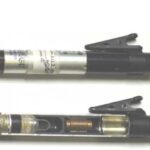
The selection of the material for the thin film detectors is critical. A range of materials, such as tantalum, tungsten, and niobium nitride, have been used to fabricate TES (Figure 2). Proper design of a TES is important, as is proper integration of the TES into an application.
Building a TES circuit
A TES is voltage-biased by driving a current source (Ibias) through a load resistor (RL) as shown in Figure 2. When properly biased, the power dissipated in the TES is constant with the applied voltage keeping it in the transition region. When the TES absorbs a photon, the added power is removed by negative electrothermal feedback where the TES resistance increases, resulting in a drop in the current and the Joule power, cooling the device back to equilibrium in the self-transition region.
Individual TES devices have typical dimensions of a few hundred microns. For many applications, arrays of hundreds or thousands of devices are multiplexed using superconducting quantum interference devices (SQUIDs). A common configuration places the TES in series with an input coil (L) inductively coupling it to the SQUID series array. Multiplexing large numbers using a SQUID array enables high-energy resolution spectroscopy. The SQUID, in turn, is connected to room-temperature electronics through an amplifier.
TES plus scanning transmission electron microscope
Astrophysicists often use an EDS together with a scanning transmission electron microscope (STEM) to analyze the abundance of an element with an accuracy of a few percentages in sub-micron scale spatial resolution.
However, the combination of an EDS and STEM is not effective for resolving emission lines at closely spaced energies. If the EDS is replaced with a TES, the resolution can be significantly improved even with high counting rates.
In one instance, a 64-pixel TES array measuring 5.2 mm square was developed for use with a STEM. The size of the TES array was constrained by the geometry of the STEM and the detector head on the 100 mK refrigerator. The new design delivered improved accuracy with systematic errors < 1%, even for closely spaced emission lines. A level of performance that’s not possible using an EDS and STEM combination.
Summary
A TES provides astrophysics with a power alternative to conventional EDS tools for resolving emission lines at closely spaced energies when analyzing the relative abundance of elements like boron, carbon, and oxygen versus silicon. In practical implementations, an array of TES is multiplexed using SQUIDs and external amplifiers to capture the signals and connect them to room-temperature metrology electronics.
References
A Concept Design of TES X‑ray Microcalorimeter Array with Different Thickness Absorber Toward the Observation from 50 eV to 15 keV for STEM‑EDS, Journal of Low-Temperature Physics
A Review of X-ray Microcalorimeters Based on Superconducting Transition Edge Sensors for Astrophysics and Particle Physics, MDPI Applied Sciences
Development of highly sensitive nanoscale transition edge sensors for gigahertz astronomy and dark matter search, Journal of Applied Physics
Transition Edge Sensors (TES), Massachusetts Institute of Technology
Transition-Edge Sensor, Wikipedia
Leave a Reply
You must be logged in to post a comment.