Micro photo sensors have built-in amplifiers and are available in a variety of configurations, with modulated, non-modulated, and polarized light beams. They’re used to provide precise and stable sensing or positioning of materials, components, or assemblies. Some have integrated connectivity, like IO-Link and IP 67 environmental ratings.
Uses for micro photo sensors include precision manufacturing equipment in Industry 4.0 factories, wafer handling in semiconductor fabrication operations, and photoplethysmography (PPG) detection of blood oxygenation (SpO2) in pulse oximeters.
This FAQ reviews various micro photo sensor designs and how they are optimized for specific applications.
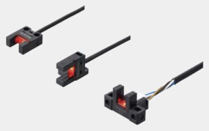
Transmissive slot micro photo sensors detect the presence of an object as it passes through the slot, or aperture, and interrupts the light beam from the emitter. In addition to object recognition, these sensors can be used for precise positioning of objects. The optical axis of the emitter and receiver are fixed, simplifying installation. These sensors are available in a wide range of configurations and connector types (Figure 1).
Through-beam micro photo sensors consist of separate emitter and receiver units. They operate on the same principle of beam interruption as slot sensors, but the emitter and receiver can be placed far apart and are suitable for applications that demand long sensing separations. Proper alignment of the emitter and receiver is critical when using these sensors.
Reflective micro photo sensors, sometimes called diffuse-reflective sensors, include the emitter and receiver in the same module. When an object enters the sensing area, light is reflected to the receiver. Some reflective micro photo sensors are designed with the ability to recognize printed markings on the packaging. Limited reflective sensors are special designs optimized to operate in the presence of background objects that could otherwise cause unstable sensing performance.

Retroreflective micro photo sensors are designed for applications that need long sensing distances. The emitter and receiver are in separate modules and require alignment for proper operation. When an object passes through the light beam from the emitter, it blocks the light from getting to the receiver and is detected. The need for accurate alignment of the emitter and receiver makes it difficult to achieve high precision with this type of sensor.
Pulse oximeter
A pulse oximeter uses the different light absorption characteristics of oxygenated hemoglobin (HbO2) and deoxygenated hemoglobin (RHb) at specific wavelengths of light. A pulse oximeter has been implemented using two LEDs, a 660 nm red LED and a 940 nm IR LED, and a photodiode receiver that operates in a reflective configuration in a highly integrated photo micro sensor.
The sensor operates in three stages. First, the red LED is pulsed, and the return signal is measured; next, the IR LED is pulsed, and the return signal is measured; finally, the background signal is measured with both LEDs off to exclude interference from extraneous light sources. The sensing function is segmented into four photodiodes that can be multiplexed into two or four separate optical channels connected to the analog signal processing block, depending on the design requirements (Figure 3).

Wafer handling
Sometimes even micro sensors are too large. In an automated semiconductor wafer fab, the wafers are moved between processing machines in specialized front-opening unified pods (FOUPS). When wafers are placed in the FOUPS by a robot handler, they may be misaligned, some slots may be empty, or some slots may contain multiple wafers. The robot handler receiving the FOUPS needs to identify missing, misaligned, or multiple wafers. Otherwise, the very expensive wafers can be damaged, resulting in significant financial losses.

The wafers in the FOUPS are only a few millimeters thick, and the wafer identification photo micro sensor must be extremely thin. For this application, a conventional micro photo sensor with a built-in amplifier is too large. Specialized micro photo sensors with an external amplifier module have been developed. These through-beam sensors consist of 1.5 mm thick transmitter and receiver units connected to the amplifier module with flexible cables (Figure 4). When installed in a wafer handler end effector, they can quickly and reliably identify correctly filled slots, tilted wafers, and doubled wafers.
Summary
Micro photo sensors have built-in amplifiers and are available for a wide range of applications. They are mostly used for object sensing and positioning, but custom designs are available for specialized applications like pulse oximeters and material handling equipment in semiconductor fabs.
References
Design and Fabrication of a Thin and Micro-Optical Sensor for Rapid Prototyping, MDPI sensors
Micro photoelectric sensors, Panasonic
Photo microsensors, Omron
PPG Optical Sensor Module with Integrated Red/IR Emitters and AFE, Analog Devices
Reliable wafer mapping, Balluff

